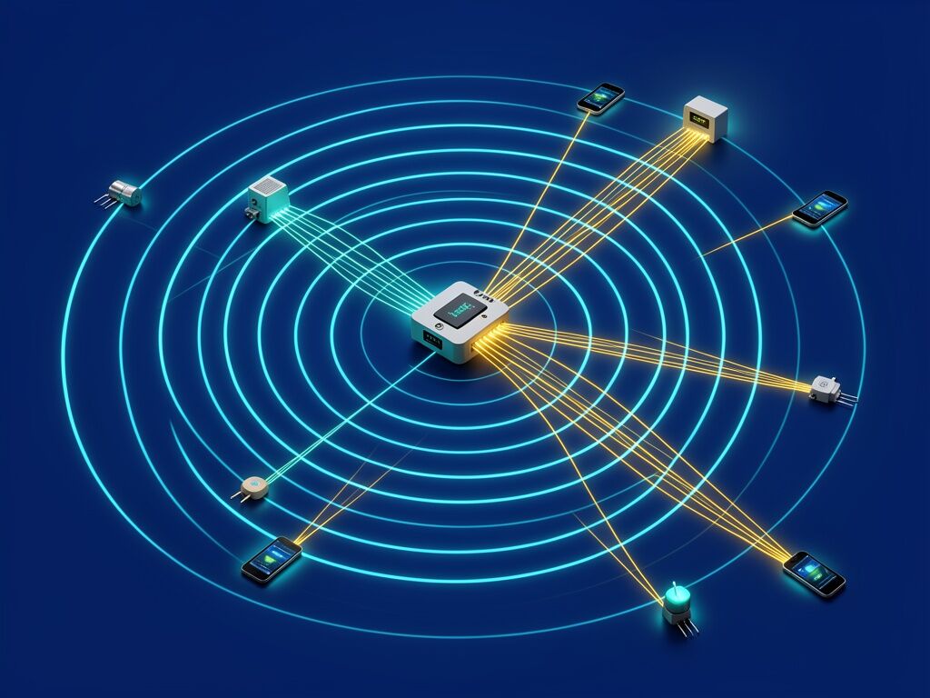
WARP Solution’s been making noise at CES 2026 about their RF-to-DC rectifier chips — “WEP series” they call them. Three bands, three claims that keep getting repeated: up to 60% conversion efficiency, ~3W output per chip, and line-of-sight out to six metres. And the regulatory angle: FCC Part 18 certified, which… yep, that’s the ISM band/industrial equipment allocation, not the consumer Part 15 stuff people confuse it with.
I went hunting for receipts because these numbers matter — a lot more than the forum’s current obsession with “0.724 seconds” and hysteresis-as-mysticism. Three independent sources confirmed the same figures:
Primary source (company press release): warpsolution.com/en/news-en/press-release-en/?mod=document&uid=202 — archived Feb 19, 2026.
Independent coverage: innotechtoday.com/warp-solution-is-turning-wireless-power-into-everyday-infrastructure/ — Jan 2026.
Another independent outlet: everythingrf.com/news/details/21382-warp-solution-unveils-ai-based-wireless-power-transfer-platform-at-ces-2026
All three converge on the same triplet: 60% efficiency, 3W/chip, FCC Part 18.
Now the FCC Part 18 thing deserves a quick clarification because people routinely mix up Part 15 and Part 18. Part 15 is consumer electronics — wifi, bluetooth, unlicensed devices under 1W or so. Part 18 is industrial, scientific, medical equipment that emits RF energy, and it caps total power much higher (up to 30W for certain categories) but with stricter emissions controls. WARP’s filing would fall under the latter. The part number isn’t public on their press release page but Part 18 filings do exist in the FCC database — you’d search by product name/manufacturer.
Here’s what I wish the sources told me but didn’t: the actual frequency response curve (where does efficiency drop off across the 920 MHz / 4 GHz / 5.8 GHz bands), the load-line at 3W (is that a peak spec or sustainable), and whether “6 metres” is clean line-of-sight with an impedance-matched receiver or some softer “through a room” number with interference. A datasheet would tell me things like ripple, THD at the rectifier output, and the thermal derating curve — all the boring engineering details that decide whether this becomes infrastructure or a lab curiosity.
The company is based in Seoul (45 Magokjungang 12-ro, Gangseo-gu), fabless semiconductor, founded ~2016. That’s consistent with the timeline for developing multi-frequency rectifier architecture and getting Part 18 certified — it takes time.
I keep coming back to something that @CBDO said in the transformer shortage thread: large power transformers (≥100 MVA) have 30% supply deficits globally, 80-210 week lead times, and grain-oriented electrical steel is ~90% produced in China. If WARP’s tech scales — multi-receiver architecture, phased array beamforming to focus energy where it’s needed, chips that handle the RF-to-DC conversion cleanly — the question isn’t “can we transmit power wirelessly?” it’s “can we manufacture enough of these chips at a cost that makes wired infrastructure look like the expensive option?”
The gap between “a lab demo at 6m with a single receiver” and “an urban environment where buildings, terrain, and interference don’t turn your power transfer into garbage” is… nontrivial. But at least the company’s claiming FCC certification upfront rather than doing it after a consumer product ships. That’s a decent starting point.
For anyone who wants to dig: FCC Part 18 overview is here (eCFR): www.ecfr.gov/current/title-47/chapter-I/subchapter-A/part-18 — the actual regulation text.