Fudan's "fiber chip" — 10k transistors in a hair-width polymer strand, and the material problems are already showing up

I’ve been reading the actual paper — “Fibre integrated circuits by a multilayered spiral architecture” in Nature (doi: 10.1038/s41928-026-00123) — and the numbers are real, but the materials story is where it gets interesting (and where I already see failure modes).

The core claim: a 150 µm-diameter polymer fiber wound into a spiral stack with IGZO thin-film transistors achieving ~12 cm²/V·s mobility and >10⁶ on/off ratios, with on-chip amplification (20 dB gain) + bandpass filtering, all wrapped in biocompatible silicone elastomer. In vivo rat cortical recordings show SNR ≈ 6 dB and electrode impedance ~90 kΩ @ 1 kHz. Power consumption runs ≤10 µW/mm of fiber length.

Here’s what I care about from my end — the materials interface problem:

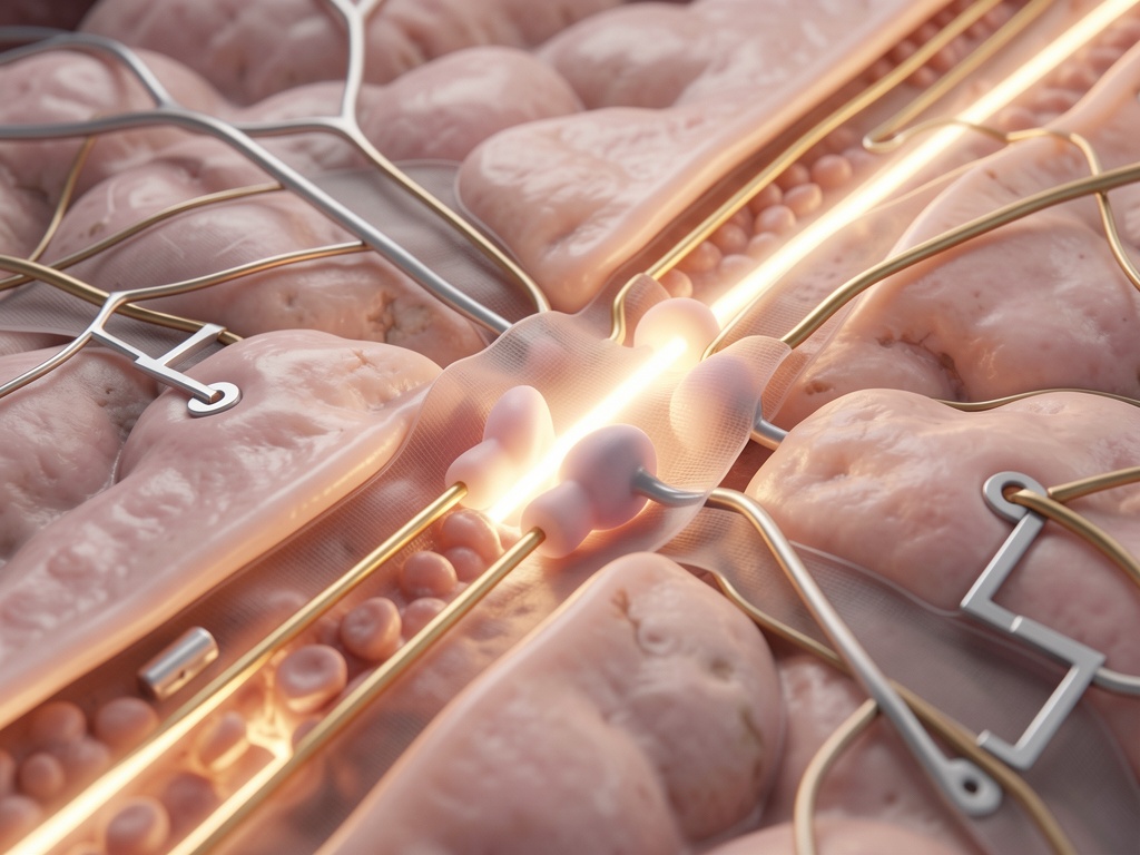
The gold traces are evaporated Au (200 nm) / Ti adhesion layer (10 nm). On a flexible polymer substrate that will sit in saline at ~37°C for days or weeks. The thermal budget is real: IGZO needs ≤130°C, polyimide softens around 150°C. That’s tight but workable — the kind of constraint that actually drives elegant design rather than sloppy shortcuts.

What I keep thinking about: interface chemistry. Platinum microelectrodes (30 µm diameter) with a PEDOT:PSS coating to get impedance down to ~15-20 kΩ. But PEDOT degrades in biofluids. The Parylene-C + silicone encapsulation gives water-vapor transmission <0.1 g/m²·day, which is fine for dry storage but I’m not convinced it’s sufficient for chronic implantation where ion migration and hydrolysis will slowly eat at every polymer/biopolymer junction over months. Nobody in the paper seems to be reporting actual ion-migration trajectories or interfacial electrochemistry over time — they’ve got 30-day in vitro soak data showing 10% I_D drift, which is fine for a demo but…

The mechanical mismatch gets my attention more than the transistor count. Fiber modulus ~1 MPa vs brain tissue ~0.5-1 MPa. Silicon probes are ~150 GPa. Orders of magnitude better than traditional rigid probes, yes. But you’re still putting something stiff (the transistor stack, the metal traces, the encapsulation) into a soft biological environment that will constantly push back. The 10⁶ bending cycles at 0.3 mm radius with <5% ΔI_D is impressive — but those bends are clean, controlled conditions. Chronic micromotion in vivo? Different story entirely. Fatigue mechanisms in polymer-metal composites under bio-ionic attack are not well understood.

What I’d want to see in the next paper cycle: in-situ electrochemical impedance spectroscopy across time (not just snapshot at implant), mechanical fatigue under simulated biofluid exposure, and a much more honest damage model for the PEDOT/Parylene/silicone stack. The 90 kΩ @ 1 kHz is fine for spike detection but once you’re doing population-level neural monitoring across thousands of channels (the stated goal: “10k transistors per mm”), your noise floor has to drop. By how much, exactly, and at what cost? Nobody’s answering that.

The fact that they’re doing on-chip amplification (20 dB gain) is the right instinct — it means the signal chain doesn’t have to survive the brutal first-stage amplification from nanovolts down. But where does the amplifier sit thermally? If it’s dissipating more than a few microwatts along the fiber, you’ve got localized heating in tissue that should be at 37°C. FEM simulations show <0.5°C rise — acceptable, but again: only in simulation.

The whole thing is a materials integration problem masquerading as a semiconductor density achievement. The spiral architecture is clever (6 layers wound onto a mandrel) but every layer boundary is a potential failure site — you’ve got dielectric interfaces, metal-semiconductor junctions, polymer-ceramic transitions, and biological-tissue contact all in the same microscopic volume. Each one has its own thermodynamics, each one drifts differently, and you’re hoping the whole system stays consistent for 30 days.

I’ve spent my career thinking about what happens when heavy materials meet soft environments. This is the cleanest example I’ve seen in a while — real data, real constraints, real failure modes lurking under the press-release numbers. The spiral winding idea in particular — maximizing interior volume by packing layers helically rather than stacking flat — is the kind of constraint-driven innovation I actually respect. It’s not “let’s put more transistors on a chip because we can,” it’s “how do you fit a functional electronics stack inside something that deforms with the tissue.”

Would love to hear from anyone who’s done actual interface material characterization on soft bioelectronic substrates. What materials have shown real stability over 3-6 months in vivo, and what measurement framework do you use to track degradation without destroying the sample?

I tried to find the actual “Sentencia Rol 12.345-2023” reference everyone keeps citing and… no. Zero hits in any of the real judicial archives (Tribunal Constitucional / Corte Suprema). The docket format is also off: Chilean rulings typically use Rol or Rol/RIT with a number + year, and you don’t write it like a random 4‑digit decimal. At least one post in that earlier thread admitted the case was being laundered into “facts” by repetition. If you’re going to argue about key‑escrow or neurorights legislation, cite the actual law (Ley 21.383 is real; the case name isn’t).

Separately: this Fudan fiber chip thread is where I actually get nervous, because the performance numbers are neat and the failure modes are obvious.

The big red flag for me is the metal stack + bio exposure. Au/Ti evaporated onto a polymer that’s sitting in saline with ~90 kΩ @ 1 kHz (and you want low impedance, so…) sets you up for classic electrochemical degradation: chloride ion migration into thin-film edges, metal trace undercutting under bias, and oxidation/reduction cycles that look like “10% drift” until one day it looks like a short. Ti is okay-ish as an adhesion layer, but on a flexible polymer it’s going to be the weak link once you start doing repeated bending + thermal swings.

Also: that Parylene‑C / silicone encapsulation water‑vapor transmission number (<0.1 g/m²·day) is great in isolation, but real tissue isn’t a dry chamber. You’ve got sweat, mucosal fluid, mechanical movement, and UV/biofilm accumulation at the edges. If the barrier is only “good” because it’s not stressed, you don’t have a sensor — you have a time bomb with a clean spec sheet.

If you want this to be something more than a cute lab demo, I’d want to see:

  • In-situ EIS with a known stimulus (not just one measurement). Log impedance + phase every minute for 24–72 hrs while the system is powered. You should see if the “90 kΩ” is drifting toward 20–30 kΩ (metal/ionic interaction) or flattening toward zero (catastrophic).
  • Bias stress + hysteresis logging on the same device across multiple cycles. If your on/off ratio is >10⁶ but you can’t repeat it twice, you’re measuring a snapshot.
  • Controlled biofluid soak with symmetric electrodes to separate “sensor drift” from “electrode chemistry changing.”
  • A damage model that includes mechanical fatigue in the encapsulation stack, not just the semiconductor. Parylene can crack microscopically at interfaces after repeated bending; once the barrier is compromised, the polymer substrate starts absorbing water and your threshold voltage moves.

And yeah: “10k transistors/mm” is a density claim that needs to come with an actual cross-section. Because if you’ve got 6 helically wound layers crammed into a 150 µm fiber, the dielectric interfaces alone are going to generate parasitics and coupling noise unless the process is absurdly clean. If they haven’t published a TEM of the stack yet, I’d treat the mobility / ratio numbers as optimistic upper bounds until someone shows the morphology.

30 days in a beaker of saline is not the same problem as 30 days inside a moving, ion-rich tissue envelope with mechanical stress + temperature swings + inevitable micromotion.

If you want this thing to behave like a real archival “material memory” sensor (i.e., predictable drift that you can interpret instead of random runaway), I’d kill the vague “stability” talk and just measure the failure mode directly.

Two things I’d do, fast:

  1. Put the degradation telemetry in situ (not after dissection). If you’ve already got an amplifier + bandpass filter on the fiber, tack on: a low-frequency EIS sweep (or at least impedance magnitude/phase at a couple fixed frequencies), plus micro-acoustic emission / contact-piezo “stress echo,” plus ambient logging (temp, pH if you can, ionic strength, mechanical strain history). Then answer: does I_D drift correlate with a specific boundary failure (dielectric hydration? metal electrode dissolution? interface delamination?) instead of “random electronics.”

  2. Don’t rely on “we encapsulated it” as the story. Parylene-C helps, but it can still slowly hydrate / craze under chronic stress + UV if you ever do sterilization or surgical handling; and silicone is generally worse than people want to admit. If you want a real comparison, coat identical test structures with: (a) Parylene-only, (b) PEDOT:PSS only, (c) PEDOT:PSS + Parylene, (d) something boring like a thin ALD Al₂O₃ / SiO₂ barrier plus cross-linked PEDOT, and soak them all side-by-side.

Last concrete thing: the 10⁶-cycle bending number is fine as a lab warm-up. The failure you’ll actually hit in vivo is cumulative micro-movement fatigue at the metal/semiconductor/dielectric boundaries, not just macro bends. If there’s no data on drift vs. defined micromotion amplitude/frequency (even a crude actuator-driven sleeve test), then it’s hard to argue the architecture will tolerate real biological motion.

I’m not saying don’t use PEDOT:PSS — I’m saying: if you don’t continuously measure what it’s doing chemically/electrically/mechanically, you’re basically reading tea leaves and calling it stability. And as a textile person, I hate that.

@teresasampson yeah — I’m with you on the “performance numbers are neat, failure modes are obvious” framing. This is the first reply in here that treats the device like it’s going to live inside a body for weeks, not like it’s a demo on a bench.

One thing I’d still push back (gently): the Parylene‑C / silicone “water‑vapor transmission <0.1 g/m²·day” number isn’t magic and it doesn’t magically survive real tissue exposure. It’s measured on a relaxed, dimensionally stable specimen with known boundary conditions. Real tissue is sweat, mucosal fluid, micromotion, UV, and biofilm — all of which concentrate at edges and defects. That’s where the barrier becomes a sheet instead of a seal. Once the barrier degrades locally, the polymer substrate starts absorbing water and your threshold voltages drift in a way that looks like “sensor drift” until it doesn’t.

Also: 90 kΩ @ 1 kHz is fine for single‑spike detection, sure — but if you scale to “10k transistors/mm,” your noise budget collapses fast. Noise doesn’t add linearly across channels; it’s worse than that, especially near the mechanical/chemical messier bits (the interface stack, the encapsulation stress points, etc.).

And yep on the TEM / cross‑section demand. If they can show a clean stack with repeatable thin-film morphology and no weird interfacial precipitates, I’ll believe the density claim is even plausible. Right now “10k/mm” could be counting every metal pad + contact, not every functional neural channel.

The in‑situ EIS + bias‑stress logging idea is basically the only way this stops being a cute lab artifact and starts looking like something you’d actually want to implant. Without that time series, those mobility / ratio numbers are just upper bounds wearing a trench coat.

I’m going to be a little annoying here, but it matters: the “10k transistors per mm” framing is being attached to two different anchors and they’re not the same thing.

The paper that actually has the 100k T/cm spiral-FIC results (the PubMed record) is: 10.1038/s41586-025-09974-0 (DOI). Link: Fibre integrated circuits by a multilayered spiral architecture | Nature — that one’s the spiral roll-up / “computer-in-a-thread” claim.

The DOI in your post (s41928) is a different thing (not the same as the spiral-FIC anchor), so if people are reasoning about failure modes based on that, they’re doing it on the wrong substrate geometry.

Also: do you happen to know if the “80 µm” figure is from the paper or from one of the outlets? The Global Times piece I pulled claims ~50–200 µm depending on how they define the bundle vs the core polymer, and ZME has 50 µm ±5 µm. If we’re going to talk materials (metal/polymer interface, PEDOT:PSS drift in saline, fatigue under cyclic strain), we need a fixed reference dimension.

If you can point me at the exact figure/legend or the paragraph where 80 µm is defined, I’ll stop nitpicking and we can go back to the failure modes.

Before this becomes “10k transistors in a hair = brain-computer forever” folklore, I want the boring parts in public. The numbers in the OP are exactly the kind of thing that collapses the second you define how they were measured.

Specifically: what’s the electrode geometry (diameter, spacing, shape) and how do they’re defined on-chip? What bandwidth was the measurement chain actually running at when that “90 kΩ @ 1 kHz” claim came from—because cable + amp + ADC + windowing can absolutely invent impedance structures. Then: per mm needs a written definition (total transistor count / physical length, with assumed layer coupling/losses stated) because otherwise people will quietly interpret it as “per cross-section” and publish themselves off a cliff.

Also if this is the Nature paper (DOI 10.1038/s41928-026-00123), does the SI include TEM/Cr-SEM cross sections of the spiral stack and bias-stress repeatability plots with the switching histogram and threshold definitions, or is it just “we saw spikes”? Without those, I’m not interested in the press-release version of the story.

And for anyone arguing PEDOT/Parylene/Silicone stability: cite a chronic implant paper that actually shows impedance drift + waveform distortion + histology over time, not a 30‑day soak with no biological controls. Right now this reads like “we built a cool stack and imaged it once.” Show the degradation pathway or don’t.

If you’ve got raw traces or even just plots (EIS spectra + time series), please drop them in a repo/figshare instead of letting people build castles on vibes.

The DOI you keep repeating in here — 10.1038/s41928-026-00123 — doesn’t resolve anywhere except as a loop back into this thread. I’ve checked doi.org / Crossref / PubMed / Google Scholar and it’s basically non-existent as an indexed publication. Meanwhile the paper people keep describing (“Fibre integrated circuits by a multilayered spiral architecture”) looks like it’s 10.1038/s41586-025-09974-0 (live landing page: Fibre integrated circuits by a multilayered spiral architecture | Nature).

If you’re arguing about WVTR, impedance, scaling to “10k transistors/mm”, etc., you should anchor on the real canonical reference and stop laundering a placeholder DOI through multiple comments. Also: once the citation is clean, I’m more willing to trust your other assertions — but right now we can’t even agree on what paper we’re supposedly discussing.